
By the Nanofabrication Core Lab team and EMG
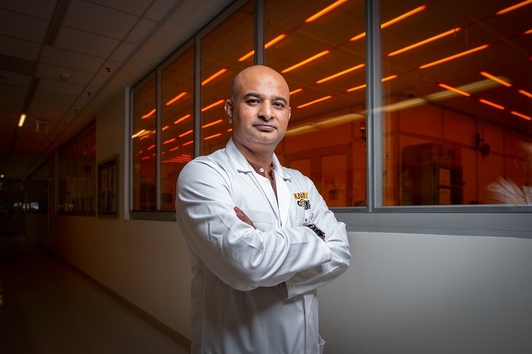
In the extraordinary world of material engineering and semiconductors, size matters—and smaller is better when it comes to nanotechnology. Materials such as very thin films have amazing properties in certain conditions that are not achieved by the bulk material. KAUST Core Labs and Research Infrastructure’s new Material Engineer Nabeel Aslam, who works in the Nanofabrication Core Lab (NCL), brings expertise in these unique areas to the University.
During his master’s degree in Pakistan in 2008, Aslam discovered nanotechnology, the incredible way materials behave at an extremely small scale. After completing his studies, Aslam worked as a technology and development engineer for a semiconductor manufacturing company in Germany, where he fabricated semiconductor chips. Every computer or smartphone is powered by the chips, which are made from a wafer of silicon covered with billions of transistors fabricated using thin film layers multiple times thinner than a strand of hair.
The thin film layers are special because they have the ability to conduct electricity more than an insulator, such as glass, but less than a pure conductor, such as copper or aluminium. They can be thought of as a kind of half-conductor—or by their real name, semiconductors. The assembly of transistors and other electronic components forms the microchips, and the semiconductor industry always aims to produce microchips that are smaller, faster, and cheaper.
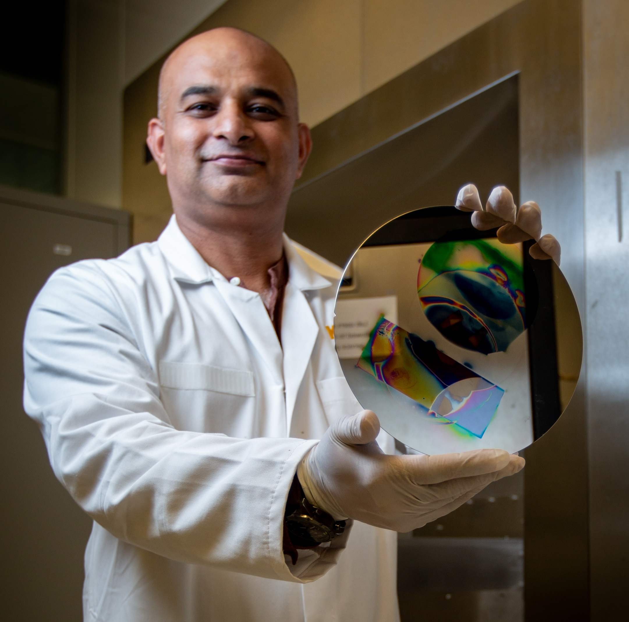
After discovering nanotechnology during his master’s degree studies in 2008, Nabeel Aslam decided to become a material engineer and focus on using new materials to create a better world. Photo by Khulud Muath.
Small is important because, according to Aslam, the key is to develop microchips that deliver high performance and high memory using low power and less space.
“In NCL, we are developing ways of fabricating electronic devices using thinner and thinner materials that are capable of delivering ever-greater memory, speed and energy efficiency,” he said. “We’re developing semiconductors on a nanoscale that can be used for photovoltaic panels for solar energy; all types of sensors for various applications; bio-sensors for diagnostics; memory chips and logical devices; or microelectronics for use in cameras and smartphones combined with the Internet of Things.”
If the nanoscale number is low (for example, 7 nanometers technology-N7—well into quantum realm—as currently used in the iPhone 12), Aslam explained, then the electrical current doesn’t have to travel as far to get to where it needs to go, requiring less power and time. This enables nanocircuits that can perform faster and more complex functions using less power. Because of this, smartphones are getting faster, smaller and more powerful, and Samsung or Apple, for example, turn to companies like Intel or Advanced Micro Devices to get the most advanced chips.
In NCL, Aslam has the opportunity to work in a research environment full of experienced scientists and professionals and cutting-edge tools, providing him with what he said is a “multi-institutional perspective.” The research part of his activities additionally gives him the ability to explore some of his favorite technologies.
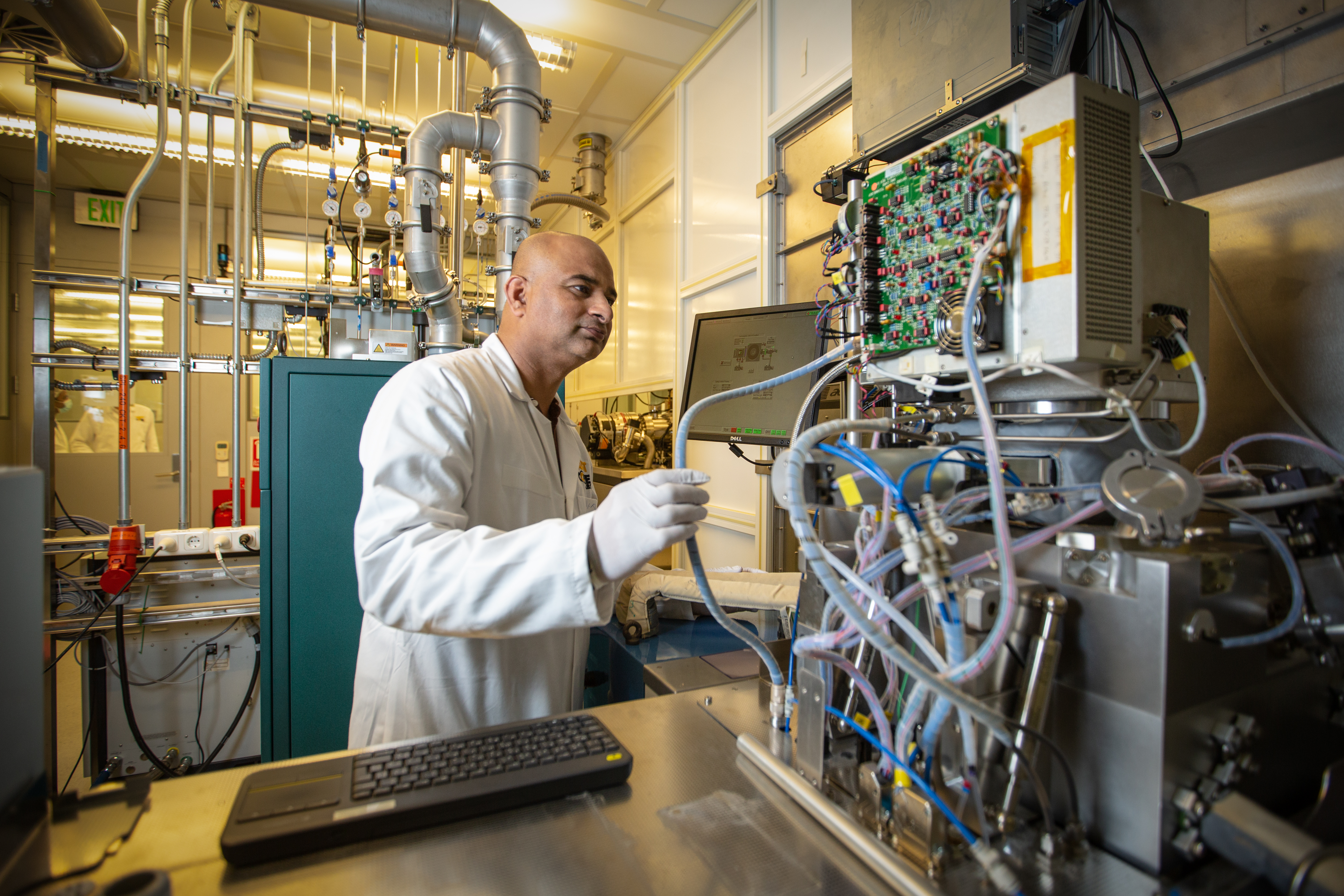
Nabeel Aslam finds creating thin films in the range of one atomic layer through atomic layer deposition to be a complex but exciting process. Photo by Khulud Muath.
“My favorite area is thin films in the range of one atomic layer,” he noted. “It’s a really exciting but very complex way of using chemical vapors to create very thin layers of film for use in semiconductors. It’s also called atomic layer deposition, or ALD, and it’s proving to be a game changer in developing objects like advanced photovoltaics; batteries; bio-sensing and diagnostics; plastics; textiles; advanced packaging; and food and corrosion protection coatings; and it is also used in the manufacture of semiconductors.”
Now that Aslam is part of NCL’s growing team of scientists, he works to push the boundaries of nanotechnology research and development at KAUST. He also focuses on his career goal of harnessing the power of small matter to make an impact on humanity.
“I know that we have the tools in our hands and the science at our disposal to create completely new materials that have the potential to transform the fields of medicine, renewables and computing to create a better world,” Aslam said. “That is ultimately why I am a material engineer and it’s why I am part of NCL and KAUST—to serve humanity.”