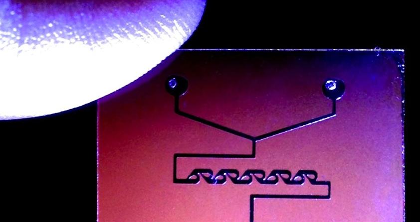
Personalized healthcare has been identified as a promising technology for health promotion and early disease detection. One day, you may not need to go to the doctor for simple blood or saliva testing. All this could be done at home using existing smartphone technology - and our scientists are helping to make that vision a reality.
Imagine attaching a sensor to your smartphone, which will analyze a tiny amount of blood or saliva, and the data output will be available via a mobile application. To make this vision a reality, microfluidics will play a major role in the process by using standard integrated circuit (CMOS) technology.
Here, in the Nanofabrication Core Lab, microfluidics devices and technologies have been developed in conjunction with faculty members across different disciplines. One of these technologies, Flash Microfluidics, could have applications in low cost, disposable microfluidics sensors for early disease detection.
To demonstrate that this will be possible, our team is fabricating devices as a proof-of-concept. The Flash Microfluidics technology we’ve developed provides a fast and economically-viable method to fabricate a microfluidics device in a single step.
Here’s how Flash Microfluidics works:
This technology is groundbreaking because it can easily seal various surfaces or components together while simultaneously building the necessary channel network for fluids to pass through a device or sensor. This technology has the added benefit of using in the process a low-cost image projector that is accessible in most offices or homes today.
More about the microfluidics facility
Our microfluidics facility also provides students and scientists other fabrication techniques such as mechanical machining on acrylic-based materials and laser etching. Thin metal layers under 300 micron can be cut by a 1micron wavelength Ytterbium fiber laser. This laser also allows for differential laser etching, so thin films of metals on polymers can be etched without affecting the polymer substrate underneath, an important requirement for advancing the studies on flexible electronics. The applications range from RF antennas to ITO removal from glass substrate for studies on solar cells. Cleaner silicon wafer dry dicing can also be performed with this laser.
Our built-in clean room is fitted with maskless lithography capabilities to fabricate microfluidics devices on silicon substrates. The silicon wafer is then anodically bonded to glass.

