
Providing expertise in the fabrication and characterization of micro- and nano-scale devices
Contact the labThe Nanofabrication Core Lab providing expertise in the fabrication and characterization of micro- and nano-scale devices. To maintain the level of cleanliness required by the cleanroom operations related to fabrication of such a small-scale structures, the requirements of specific standard ISO 14644 are strictly observed and enforced, special attention being directed toward actions to avoid/minimize contamination.
Watch Video
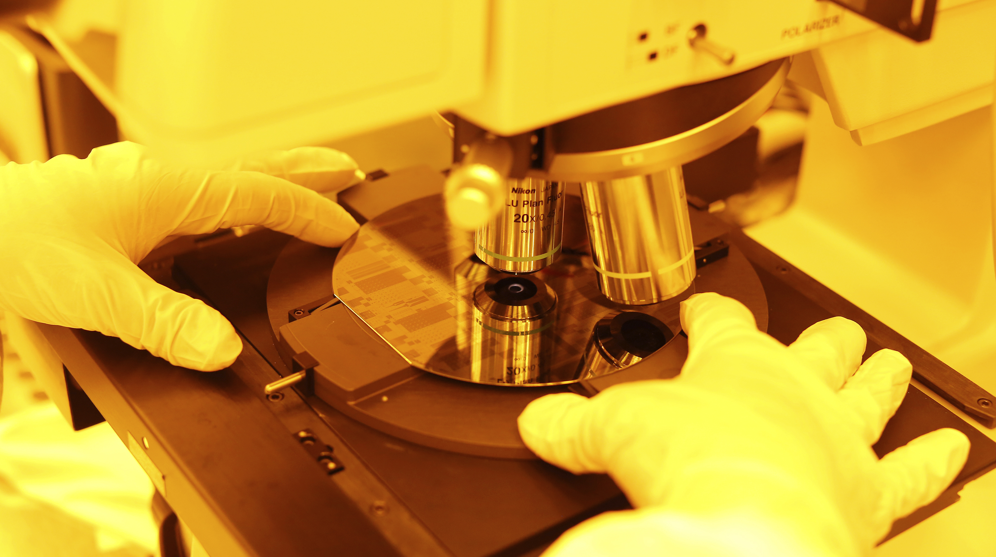
Metrology is the science of measurement, and it is employed in characterization of structures and devices to ensure device fabrication is in accordance with design. This area is equipped with versatile facilities for metrology and packaging of semiconductor devices, such as thickness measurement, profilometry, optical properties, 3D imaging, conductivity and thin film stress measurements. After fabrication, the chip has to be packaged for use outside the cleanroom. We have the capability to dice wafers down to 1 cm by 1 cm chips with our diamond dicing equipment and gold/aluminum wire bonders, facilitating successful electrical connections with the external characterization electronics.

For a listing of capabilities available in this area please click here
Dry and wet etching facilities are available for the total or partial removal of layers from the surface of materials. The Cleanroom is equipped with plasma etching equipment that are connected to reactive gasses (fluorides and chlorides), and can be used to etch more than fifty different types of materials. We provide ion beam (argon-based) etching which can produce sub-micron dense and isolated features with minimal edge roughness. We also provide wet benches with various chemicals which can be used to etch metals, semiconductors and insulators. Pre-clean benches are available for preparing wafers before processing, to ensure minimal contamination.

For a listing of capabilities available in this area please click here
The microfluidics lab offers to users a variety of techniques for the fabrication of microfluidic systems. These include thermal bonding of acrylic parts, surface activation of glass and PDMS, and anodic bonding of glass wafers to Si wafers. A method has been developed and patented for KAUST to speed up the fabrication process of microfluidics devices using a 3D resin and a projected image setup.
Other capabilities include screen printing on polymers, silicon wafers or glass for solar cells; chrome mask patterning in the cleanroom attached to the lab; and laser processing of polyamide surface which turns into graphene and can be used for electrolysis purposes, super-capacitors, batteries and bio-sensors. Paper-based flexible electronics can be fabricated very quickly using laser patterning in a two-step process developed in the lab.

For a listing of capabilities available in this are please click here
The modern semiconductor integrated circuits production involves thousands of processing steps and can be compared to constructing a building floor by floor and room by room.
Many of these steps involve the deposition of conducting, semiconductor or dielectric layers. We have the capabilities for thin films deposition with thickness starting from one single atomic layer with excellent uniformity and stoichiometry.
Thermal diffusion at elevated temperature (>800°C) is employed to diffuse n-type and p-type doping elements through bulk silicon or glass. Rapid annealing is also available.

For a listing of capabilities available in this area please click here
The Thin Films lab is a thin layers growing and characterization facility to support the fundamental and applied research of the physical and chemical properties of films and their relevant applications such as; optical, catalytic converters, magnetic, ferroelectric and spintronic devices, magnetic sensors, and carbon nanotube transistors. We have the capabilities to deposit thin films by physical and chemical vapor deposition starting from thickness of one single atom layer.

For a listing of capabilities available in this area please click here
Lithography is employed to define microscopically small patterns, structures, and devices on to wafers and allows for fabricating as many as 10,000 transistors on a 1 cm by 1 cm chip. Our capabilities include among others optical photolithography with a mask resolution of 700 nm, electron beam lithography for patterning features as small as 10 nm and two-photon laser lithography for printing 3D nanostructures with micron-range dimensions.

For a listing of capabilities available in this area please click here